
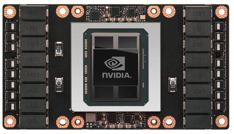
Today at GTC 2016 NVIDIA has just unveiled its fastest GPU to date in the brand new GP100, which is based on the company’s next generation Pascal architecture. The GP100 is NVIDIA’s most advanced CPU to date and will power the company’s Tesla P100 graphics card, which was also just announced.
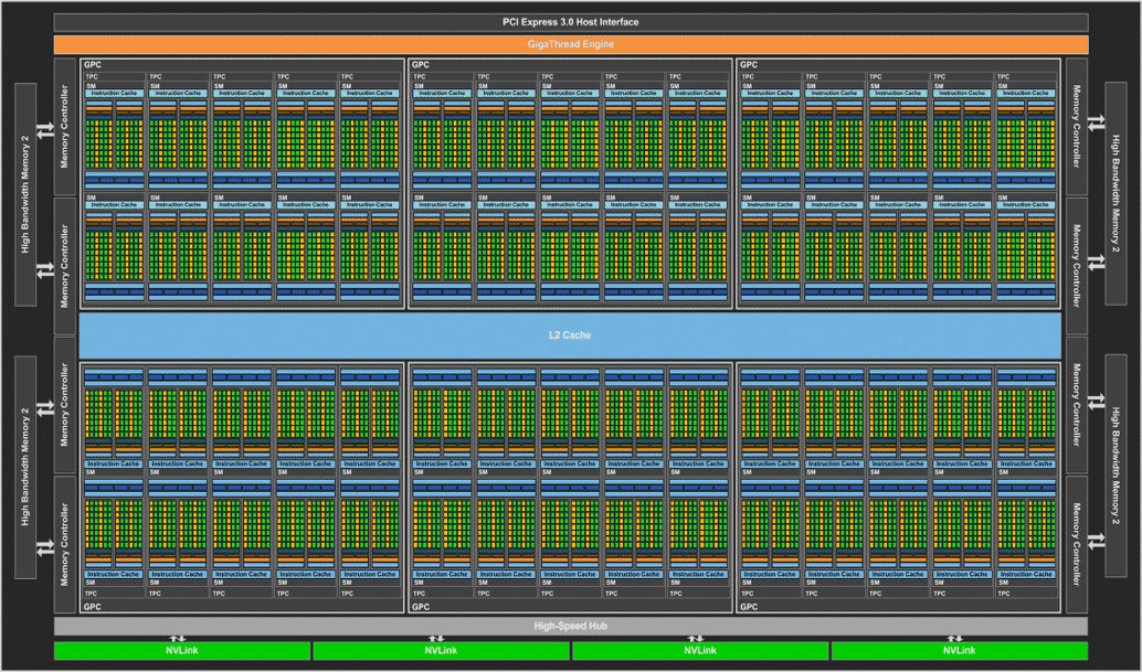
NVIDIA says that the GP100 is the largest FinFET GPU that has ever been made, measuring in at 600mm² and packing over 15 billion transistors. The GP100 is a new multi-chip module, with a layout that is very similar to AMD’s “Fiji” GPU. The GPU die sits on top of a silicon wafer, through which a 4096-bit HBM2 memory interface wires it to 3D HBM2 stacks.
NVIDIA Pascal GP100 Specifications
The GP100 GPU is comprised of 3840 CUDA cores, 240 texture units and a 4096-bit memory interface. The 3840 CUDA cores are arranged in 6 Graphics Processing Clusters, or GPCs. Each of these have 10 Pascal Streaming Multiprocessors.
Each Pascal streaming multiprocessor includes 64 FP32 CUDA cores, half that of Maxwell. Within each Pascal streaming multirprocessor there are two 32 CUDA core partitions, two dispatch units, a warp scheduler and a fairly large instruction buffer, matching that of Maxwell.
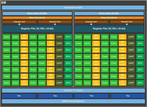
The GP100 GPU has significantly more CUDA blocks than Maxwell. This is because each of these has access to a register file that’s the same size of Maxwell’s 128 CUDA core SMM. This means that each Pascal CUDA core has access to twice the register files. This means that we should see even more performance out of Pascal CUDA cores compared to Maxwell.
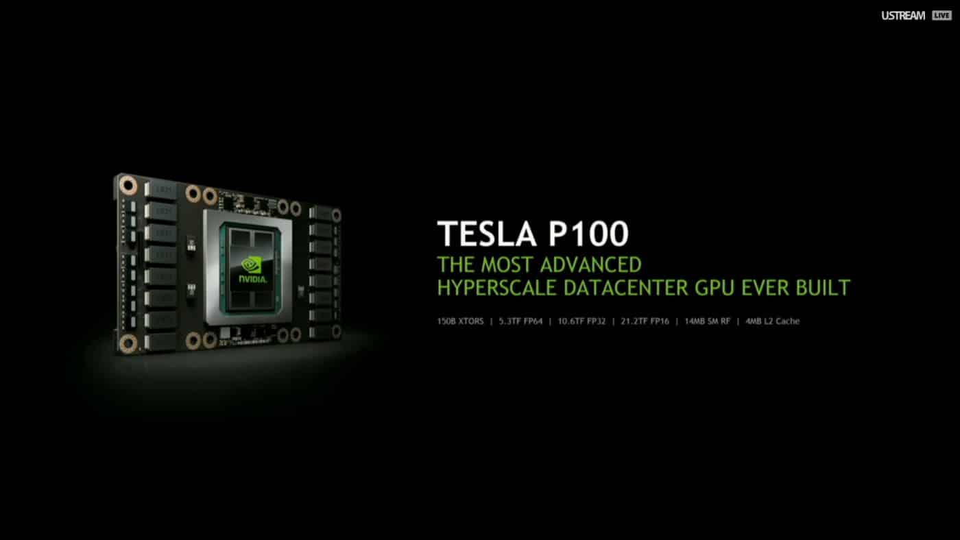
The first graphics card that will be based off of the GP100 will be the Tesla P100, which is an HPC board. So it looks more like a compact module than a traditional graphics card. The P100 offers a double-precision (FP64) compute performance of 5.3 TFLOP/s, FP32 performance of 10.6 TFLOP/s, and FP16 performance of a whopping 21.2 TFLOP/s. The chip has registers as big as 14.2 MB, and an L2 cache of 4 MB. In addition to PCI-Express, each P100 chip will be equipped with NVLink, and in-house developed high-bandwidth interconnect by NVIDIA, with bandwidths as high as 80 GB/s per direction, 160 GB/s both directions. This allows extremely high-bandwidth paths between GPUs, so they could share memory and work more like single-GPUs. The P100 is already in volume production, with its target customers already having bought it all the way up to its OEM channel availability some time in Q1-2017.