
NVIDIA’s GeForce GTX 900 series graphics cards will be launching this week and we wanted to give you a preview of what to expect from NVIDIA’s latest graphics cards. Both the GeForce GTX 980 and GeForce GTX 970 will be based off NVIDIA’s GM204 silicon. We have already seen the Maxwell architecture on NVIDIA’s entry-level GM107 based cards, the GeForce GTX 750 Ti and GeForce GTX 750. Now it is time for the performance segment cards, which will include the GTX 980 and GTX 970 to start with the GTX 960 to come later down the line. We have compiled all of the information we know about both cards in this article. We will keep this article updated as more information comes available.
Last Update: 9/18/14 @ 1:08 PM EST
NVIDIA Maxwell GM204
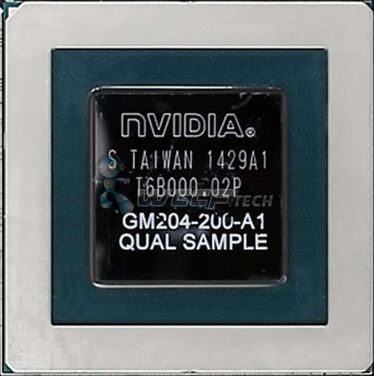
Above is the first die shot of NVIDIA’s Maxwell GM204 chip. This chip will be used in both the GeForce GTX 980 and GeForce GTX 970. For those who don’t know Maxwell is the successor to the Kepler microarchitecture. With Maxwell, NVIDIA introduced an all-new design for the Streaming Multiprocessor (SM) that dramatically improves power efficiency. So it is expected that these new graphics cards will be less power hungry and more efficient.
NVIDIA’s GM204 is the first GPU based on NVIDIA’s second generation Maxwell architecture. Many people expected a smaller fabrication process, but the GM204 is based on the 28 mm fabrication process. GM204 has four Graphics Processing Clusters (GPCs), each with four Streaming Multiprocessors “Maxwell” (SMM). There are four 64b memory controllers and the large L2 cache is accompanied by 64 ROPs. For those wondering the L2 cache is 2MB.
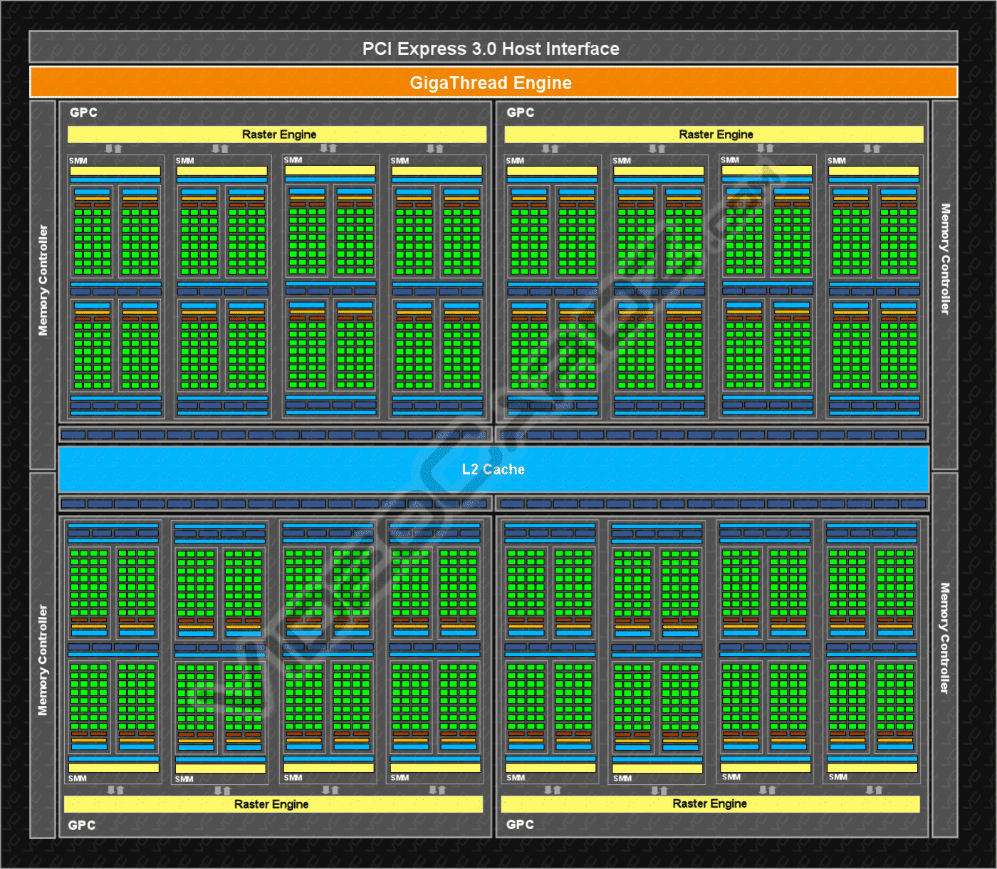
The 400 variant of the GPU that is going to be used in the GeForce GTX 980 has 16 SMMs. The big change here is that GM204 will have 64 Raster Operating units (ROPs), that’s more than Kepler GK110. The GM204 has the same number of Texture Mapping Units (TMUs), but since it has a higher clock the texture fillrate is actually higher. GM204 has 5.2 billion transistors and has a die size of 398 mm2.
NVIDIA is advertising some new technology with GM204, the first is Dynamic Super Resolution. This is new upscaling technology that is being called “4K quality on a 1080p display”. Next we have Third Generation Detal Color Compression. This is said to help with memory efficiency. Finally there is Multi-Pixel Programmable Sampling technology which improves sample randomization and reduces quantization artifacts.
NVIDIA GeForce GTX 980
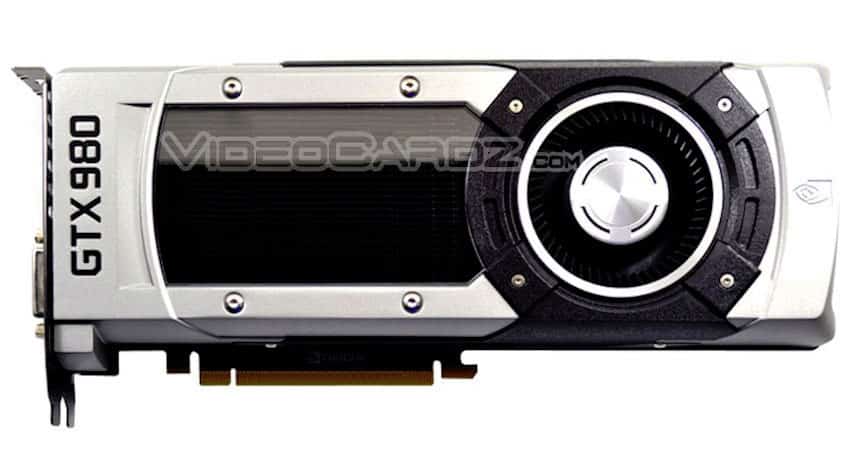
Before we get into the specifications of the GeForce GTX 980 I wanted to point out one main difference with this card. NVIDIA is trying to help us out by phasing out DVI, which has been around since we saw the first flatscreen displays. NVIDIA is now promoting DisplayPort, which the GeForce GTX 980 has three DisplayPort ports along with HDMI and a single dual-link DVI port.

Below is a full list of the GeForce GTX 980’s specifications. The big thing to point out here is that the card will have 2048 CUDA cores, 128 TMUs and 64 ROPs. The card will come with 4 GB of GDDR5 memory across a 256-bit interface. The GTX 980 will have a base clock of 1126 MHz with a boost clock of 1216 MHz. All of this at a TDP of 165W. The card has HDMI 2.0 support.
Codename: GM204
GPU Core: Maxwell
SM Units: 16 x 168
CUDA Cores: 2048
ROPs: 64
TMUs: 128
Core Clock: 1126 MHz
Boost Clock: 1216 MHz
Memory: 4 GB GDDR5
Memory Bus: 256-bit
Memory Clock: 7.0 GHz (effective)
TDP: 165W
Display Output: 3x DisplayPort, HDMI, DVI
Power Connectors: 6+6pin
Launch Date: September 19th 2014
Price (expected): $599
NVIDIA GeForce GTX 970
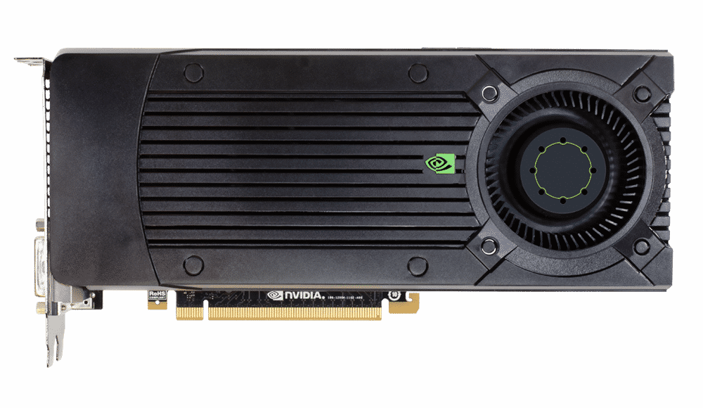
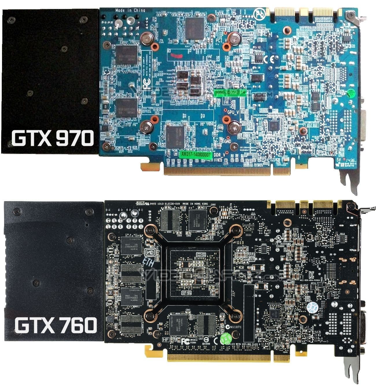
Here are photos of a reference GeForce GTX 970 card. Of course being a reference card it is not much to write home about, but that is because NVIDIA will not be shipping reference-designed cards. The GeForce GTX 970 will most likely be an AIC-exclusive, meaning that you will only find custom-designed cards based on this chip. Looking at the reference PCB we can see it looks like the same one that NVIDIA used on the GeForce GTX 760, GTX 670 and GTX 660 Ti. This is because the GK104 and GM204 are actually pin-identical. We have seen this in the past from both AMD and NVIDIA.
Now for the specifications…
Codename: GM204
GPU Core: Maxwell
SM Units: 13 x 168
CUDA Cores: 1664
ROPs: 32
TMUs: 104
Core Clock: ~1051 MHz
Boost Clock: ~1178 MHz
Memory: 4 GB GDDR5
Memory Bus: 256-bit
Memory Clock: 7.0 GHz (effective)
TDP: ~150W
Display Output: 2x DVI, HDMI, DisplayPort
Power Connectors: 6+6pin
Launch Date: September 19th 2014
Price (expected): $399


4GB memory nice, will two 970s run on 850w PSU?
my specs
i7-3770k
sabertooth z77
h105 cpu cooler
corsair vengeance 16gb 1600mhz ram
256gb ssd
1tb 7200rpm
It’s going to run onj idle but under load the 2 gpus will need more watts than you can give to them..Take a 1000w or a 1200w psu
well i asked the question on toms hardware, at full load it only uses like 600 watts