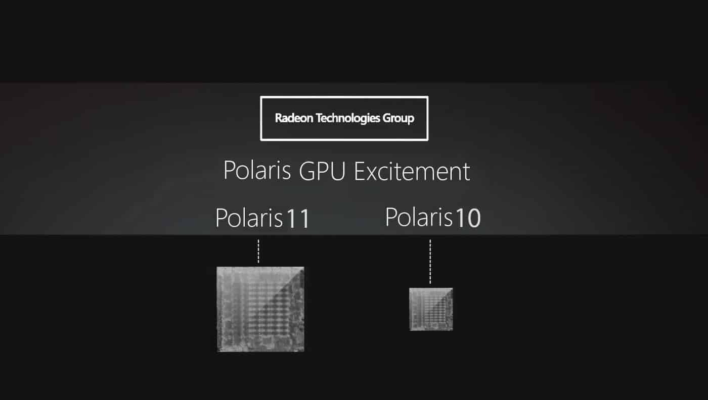
We now have some pretty solid details on AMD’s upcoming 14nm Polaris GPU. The information comes from a LinkedIn profile of a former senior engineer at AMD. On his LinkedIn profile he mentions details of various chip projects he was involved in. Project “F” listed on his profile draws attention as it is a graphics chip with a die-area of 232 mm², 430 function blocks, built on the 14 nm LPP process.
So how do we know this is a Polaris chip? Well first it is based on the Samsung / GlobalFoundry 14nm FinFET LPP node, which is what we know AMD will be using for Polaris. Secondly it says dGPU, which AMD is not working on any other 14nm GPU right now. Here is the screenshot of the AMD employee’s LinkedIn profile:
It is speculated that this chip is indeed a version of Polaris, a likely a performance-segment chip.
Source: WCCFTech | News Archive


